Showing posts with label MC6809. Show all posts

Saturday, March 19, 2022

Reverse Engineering MC6809 SBC... The Easy Way!

I previously documented my ultimately successful attempt to reverse engineer the CMS 9619 Advanced Single Board Computer. The main goal was to get a memory map of the system, including I/O addresses. Having this memory map makes disassembling the firmware on these boards much easier. The process I used prevously was labor intensive, and required me to:

  1. figure out what each of the pins on the PAL IC (that decodes the addresses) connects to;
  2. lookup datasheets to see if it is an input or output pin;
  3. build a small circuit to increment through all of the possible inputs;
  4. write a program to display all of the actual outputs for those inputs.
This took a lot of work and most of it is will only apply to the particular address decoder I was working on.

Ideally, I would want to just keep everything connected in circuit and just have the processor increment through all of the address lines for me, like a 16 bit binary counter. Hmm... Fortunately, the MC6809 has just such a feature built in! The "HCF" (Halt and Catch Fire!) instruction will halt the processor and increment the MC6809 address lines while holding R/W' high, causing it to output every possible address, and select every I/O chip on the board. This is perfect to build a memory map. Even better, since just one instruction does all of this, all I need to do is wire up that one instruction on the data bus and let the processor do the rest. I don't even need to program an EEPROM! Then, I can just observe the addresses and I/O enable lines using a cheap (under $10) logic analyzer. I could even use an Apple II (or another 6809 SBC) with a MC6821 PIA (or MC6522 VIA) to track the signal changes.

In the end, I decided to just program an EEPROM with a lot of HCF instructions: % touch HCF.bin % os9 padrom -c=205 8192 ./HCF.bin % minipro -p AT28C64 -w ./HCF.bin % xxd -s $((16#1FF0)) ./HCF.bin

00001ff0: cdcd cdcd cdcd cdcd cdcd cdcd cdcd cdcd
and I used my cheap logic analyzer to check the addresses and the chip select pins on the various I/O ICs on the board. Although this took a couple of steps (A15-A9 addresses, then A8-A2 addresses, before settling on A11-A8 with 4 chip select lines), I think it was probably faster than building a cable to connect to the Apple II APIO (MC6821) card, and I am pretty sure the Apple II could not have polled the lines fast enough.
Note channels 3-7 (A11-A7)incrementing nicely with HCF instruction

Wednesday, March 16, 2022

MIKUL 6809-5 Processor and Video Board

I recently procured another EXORbus processor board, the MIKUL 6809-5, for a reasonable price. Let's take a look...

Notable ICs:

  • Motorola MC6809 processor
  • MC6821 Peripheral Interface Adapter (PIA)
  • MC6847 Video Display Generator (VDG)
  • Z0844206 SERIAL INPUT/OUTPUT CONTROLLER (SIO/2)
  • MM74C923 20 Key Keyboard Encoder

Ports:

  1. EXORbus card edge
  2. RS232 and RS485 / multidrop LAN port?
  3. 20 key matrix keypad
  4. LED indicator ?
  5. video output
  6. composite video

It is interesting that the board uses the MC6809 CPU with a MC6847 VDG like the Radio Shack Color Computer (CoCo). Unike the CoCo, it does not have an MC6883 SAM, making it similar to the Radio Shack TRS-80 MC-10 (which uses an MC6803, rather than the MC6809). So the basic CPU and video chipset places it somewhere between those two computers.

Notably, the board does not have any provision for ROM or application RAM on it. As a result, it needs another memory board on the bus to function properly. The MIKUL 6218 would make a perfect companion for it, but I already modified my 6218 board to work with the my CMS processor boards...whoops. So, with the price of these MIKUL boards dropping due to an apparent glut of them, I picked up a fresh MIKUL 6218 for ~$35 and installed them both in my EXORbus MULTI-PLANE backplane.

Despite the interesting video output, I am not in love with the features. The MC6821 PIA is dedicated to running the keypad encoder and baud rate dip switches, so it can't be used for much. Really the MIKUL 6809-4 or 6809-6 (Motorola MicroModule clone?) would be a better choice as a all-in-one SBC. However, the 6809-5s are definitely more pentiful and far cheaper right now, so maybe somebody else can make use of any info I publish about it.

More details below...

Thursday, April 23, 2020

OS9 shell on a real CMS 9619!

I finally got it working thanks to the advice of a kind member of the Tandy Color Computer (CoCo) discord channel. Interrupts! Once I connected the 6551 ACIA's IRQ line to the 6809's IRQ (using the CMS 9619's TS8 jumper block), the OS9 shell came alive:

You can see the system start up with the ROM's "DEBUG19" prompt. Then it proceeds to:

  1. clear some memory
  2. use the edit memory command to enter in the ZMODEM program and a mini boot-loader
  3. jump to the boot-loader to get the first part of the kernel into memory sector by sector from a disk image
  4. jump to the NitrOS9 Kernel.
  5. The kernel starts loading in more sectors using its ZMODEM boot module, until it finally runs the terminal shell and gives me an "OS9:" prompt.

And now, with interrupts enabled, the shell responds! Now I need a proper ZMODEM file manager to load in and run other programs.

Tuesday, April 21, 2020

Fortunately... Unfortunately...

While I was waiting for my RAM to arrived, I tried burning an EEPROM for NitrOS-9 so that I could make the load time shorter and avoid the relocation problems I thought I was having. Well, it did not work.
Filled up Sockets! This would have cost
many hundreds of dollars back in the day.
Fortunately, my SRAM chips arrived early, so I got to work on installing them. Since the board expects EPROMS where I am putting the SRAM, I had to remove some jumpers that disabled writing to the sockets. I felt bad removing the beautifully wire-wrapped jumpers and replacing them with plastic jumpers, but it is for a good cause. With writing to the SRAM enabled, I tried booting. I thought it worked perfectly at first, but I realized I had run my expect script for the emulator instead of the real board. When I ran the correct script, I was sorely disappointed to find that everything was getting stuck just before the kernel was supposed to get loaded. After a lot of debugging, I figured out the problem. I had padded out the boot modules to align with the beginning of memory pages so that everything was easy to debug and compare to the source listings. Unfortunately, the emulated MC6809 was much more tolerant of scanning past the fill characters than the real MC6809. Once I got rid of the padding, everything started working... to a point. Where I was supposed to be greeted with the NitrOS-9 startup screen, I was getting gibberish:

Fortunately, this particular type of gibberish is recognizable as a baud rate mismatch, which makes sense. NitrOS-9 uses a completely different system for getting the baud rate than the CMS 9619 uses. After an adjustment to the terminal description files, I had an improvement:

YES! I was so excited until I hit the return key and... nothing. It does not respond with another prompt or an error or anything. Just stuck. More work to do...


Sunday, March 22, 2020

Setting a Real Time Clock with ZMODEM

I have had a little extra time lately since I don't have to commute for a while, so I pulled the CMS boards out of their storage boxes. One of the the things I really wanted to test out on real hardware is a routine I developed for setting the real time clock on the CMS board. Since my MC6809 ZMODEM routines are working pretty well, I decided to try out sending a command over ZMODEM, instead of a file.

Basically, if the receiver allows it, a ZMODEM sender can send a command for the receiver to execute. With the right flags, the standard lrz program will execute the commands in the system shell. Unfortunately, the receiver does not respond with the results of the command - it is not part of the protocol, since it is a receiver. But, the protocol allows you issue a command to start a ZMODEM send process to send the results, stored in a file, back to yourself! So, if I have the CMS 9619 send a ZMODEM command like this: date "+%y%m%d %H%M%S">/tmp/date.txt; lsz -y /tmp/date.txt

My terminal computer will get the date and time in the CMS 9619's expected format and save it to a file. Then, as ordered, it starts the lsz ZMODEM sender program, and sends the file contents back to the CMS 9619! The sender and receiver temporarily switch places to transfer the date string. Then the debug ROM's standard time setting routine is run to load the time into the RTC. It seems weird but it is the result of a very flexible protocol.

Now, ZMODEM does include an extension to get the system date, but it is sent as seconds since the Unix epoch. Converting that to an actual date and time without the proper libraries in 6809 assembly was beyond my skill set. Instead, the terminal (my MacBook Air) can do all of the work.

With gnu screen running on the terminal computer it is all pretty much automatic:

The screenshot of the session with the CMS9619 shows:

  1. set the incorrect time
  2. verify it is wrong
  3. run the ZMODEM command routine, which instructs on how to start lrz
  4. screen automatically starts lrz on my terminal
  5. everything completes
  6. checking the time with the "T" command, shows the correct date and time for the RTC!

Now to get the board setup to run NitrOS-9!

Sunday, March 15, 2020

NitrOS9 on (an emulated) CMS 9619

I have been working on some ideas to expand my CMS 9619 SBC. I thought an SD card interface would be a nice option, but I didn't want to use any modern microcontrollers or FPGAs. I had a circuit pretty much worked out, but then thought a Compact Flash card would work better for 8 bit transfers.

While working on a circuit to interface with the MC6821, I realized that I already have a nice RS232 connection to the computer, why not use it? So, I wrote a 6809 assembly tool for the CMS 9619 debugger (debug19) to download blocks of data using the zmodem protocol.

This was working so well, that I figured I could use it to boot load NitrOS-9 on the board. Since I am moving soon, my computers are all packed away, but I couldn't wait to try it. I made some changes to sbc09, a simple 6809 emulator, to emulate the CMS 9619. Here is a video of the boot process to NitrOS9 all the way to the shell:

And it works! I need to finish a real zmodem driver to get it running other commands on the disk image though. Once I move, I can test it out on a real computer.

Monday, July 29, 2019

CMS 9619 SUCCESS!

With the the power and serial port breakout boards hooked up, I tried turning on the CMS 9619, with no luck- nothing from the serial ports. The ROM I received with the unit is set up to run some user code on the second ROM at start-up, skipping the debugger. So, I made a patch to the ROM to make sure that the reset vector points to the debugger init code. The update has now been committed to the CMS_SBC GitHub code archive.

Unfortunately, this 2 byte change took several hours to get into an EEPROM, since I only have my Apple IIe and a Super Serial Card (SSC) to use as an EEPROM programmer. I had to make some changes to the BASIC EEPROM programmer script (Read More to see the program). I modified it so that it allows me time to switch in each 2K bank of the 8K EEPROM. Then I made the mistake of trying to upload the hex dump using a terminal connection to the Apple IIe (using another SSC with the standard ROM). Even at 19.2K bps, it took over an hour due to an overly conservative text pacing setting. I'm not sure why it took so long, but, of course, I soon realized that I had forgotten to move the jumpers to allow the programmer SSC to write to the EEPROM. The jumpers where located under my bank-switching adapter board, so I had to shut everything down to reach them. Then I discovered an off-by-one error in the BASIC code and had to start the upload over. Switching to the method I previously described by using c2t to encode the ROM hex dump, then using the Apple //e's cassette input port made things go MUCH faster.

Slow serial upload to Apple IIe System Monitor

After installing the new ROM and powering on the CMS SBC, I still did not get anything from the serial ports. Some voltage testing led me to discover that the +12V was not making it to the RS232 receivers. I had hooked up the power to an ambiguously marked (and fortunately unused) pin 'U' rather than pin 'T' on the extension board.
With power now going to all the right places, I was shocked to be greeted by:
DEBUG19 :
It worked! But it did not seem to be accepting any input. As it turns out, my wiring to the serial port adapter was slightly wrong in implementing a cross-over cable. After referring to a nice diagram online, and moving my Carrier Detect lines, it started accepting input!
APPLE IIe terminal connection to CMS 9619

Here are some of the commands I had a chance to disassemble and use ("H" is a hex digit):

  • R - Display the 6809 registers.
  • P - Enter the EPROM programmer.
    • STAT for status.
    • EXIT to quit.
  • T - Show the time from the RTC.
  • S - Set the time for the RTC. Format: "S YYMMDD HHMMSS"
  • E - Edit Memory. Format: "E HHHH"
    • Responds with "HHHH HH"
    • Enter: "HH" to set the hex value in memory.
    • [space key] for next byte.
    • "-" to go back a byte.
  • V - View Memory. Format: "V HHHH HHHH"
  • M - Move Memory. Format: "M HHHH HHHH HHHH", Source, Destination, Length.
  • G - Go to Memory (run). "G HHHH"
  • C - Clear Memory. Format: "C HHHH HHHH"
  • DI - Disassemble Instruction. Format: "DI HHHH", subsequent DI disassembles next address.
  • DB - Disassemble Block. Subsequent DB disassembles next block.

I very happy that this finally worked. It goes to show how useful an old Apple II is: I used a Centronics printer card to figure out the scheme of the PAL address decoder, a Super Serial Card to download the EPROMs and program the EEPROMs, and settled on the cassette input port to upload data. Now, to figure out something useful to do with the MC6809 SBC!

Check out all of the related blog posts for more details.

Friday, May 24, 2019

CMS SBC ROM Disassembly

Continuing my reverse engineering efforts on my CMS 9619 and 9609 SBCs, I downloaded the ROMs that were still in two of the boards. I inserted the ROMS into an Apple IIe's Super Serial Card (SSC) ROM socket, and transferred the data using the Apple IIe hardware monitor. I used a similar technique previously to program EEPROMs on the Apple IIe. However, since these are 8K ROMs, rather than the SSC's 2K ROMs, I had to solder up a little adapter board with two switches to switch in each 2K bank.

27C64 on adapter in Apple SSC27C64 adapter back side

With the ROM data in hand, I began machine code disassembly. Unfortunately I don't know 6809 assembly code, but with the help of the source code from an earlier version that I found online, I was able to figure out a lot of it. I started a new CMS_SBC GitHub project to keep the code in. It includes a makefile that translates the original Apple IIe monitor dumps into a hex dump, then a binary, then disassembles it.

Also, DaveW was kind enough to scan and post his documents for a CMS 9639 SBC that he has. It is more advanced than the 9609 and 9619 that I have, and includes an MMU. Great information there that I will need to spend some time looking at.

Friday, May 10, 2019

CMS 9619A SBC

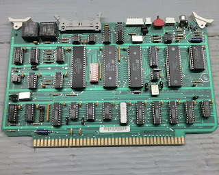
I recently came into possession of a CMS 9619A Advanced Single Board Microcomputer. I have been unable to find any authoritative information on the device, but from what I can tell, it appears to be a Programmable Logic Controller for industrial applications. It features:

  • Motorola 6809 processor - 2 MHz MC68B09
  • 3* 6821 PIA - 2 MHz MC68B21
  • 1* 50 pin header for PIAs
  • 1* 6840 PTM - 2 MHz EF68B40
  • 2* 6551A ACIA - S6551A
  • 1* 26 pin header for ACIAs & PTM
  • 5* DIP28 RAM/ROM sockets
  • Motorola "EXORbus" compatible

The board was apparently made by Creative Micro Systems which was based in Los Alamitos, California (thanks for the info DaveW). There are a number of accessory boards available, and even some early MC6800 boards that I have seen. If anyone has more information about the board, please leave a comment!

Consumer retro-computer products are the subject of massive amounts of online data, scanned manuals, and schematics, but industrial controllers have very little information available on them. Probably a lack of nostalgia or general interest combined with continuing trade secrets. But this board looks like a very capable SBC just waiting to be put to good use. So, some reverse engineering is in order. I have been saving my notes in a Google Sheet available for public view.

Serial Terminal

I think that my best chance to figure this thing out is to connect to the serial port and see if there is an interface available there. Unfortunately, the 26 pin header is not a standard DB25 header for a RS232 connection. After much continuity testing, I finished the serial/timer header pinout, which is basically:

             P1 HEADER
              ______
U27-9  CTS2  |1    2|  DCD2 U27-16
U27-11 DTR2  |3    4|  RxD2 U27-12
U26-11 DTR1  |5    6|  DSR2 U27-17
U26-17 DSR1  |7    8|  TxD2 U27-10
U26-12 RxD1  |9   10|  RTS2 U27-8
U26-16 DCD1  |11  12|  TxD1 U26-10
U26-9  CTS1  |13  14|  RTS1 U26-8
       GND   |15  16|  GND
U28-7  C3    |17  18|  GND
U28-6  O3    |19  20|  C1   U28-28
U28-5  G3    |21  22|  O1   U28-27
U28-2  G2    |23  24|  G1   U28-26
U28-3  O2    |25  26|  C2   U28-4 
             |______|

Memory Map

The CMS 6919A has a PAL IC at U12 which decodes the addresses and enables the ROM and I/O ICs at the right time. I don't have the hardware to properly reverse engineer this PAL. But, I don't really need all of the details of the PAL, just the addresses when it enables most of the ICs. I do have an Apple II APIO printer interface card which sports its own 6821 PIA, and a "General" interface to all of the PIA's pins, which should work nicely to help decode it.

I soldered up a small carrier for the PAL and a binary counter IC to deal with the high address lines since I only have 8 output bits, and the PAL accepts 11 address lines (A5-A15). I also needed to add some switches to disable the PAL until the PIA is set up properly to avoid bus contention. Without that, the PAL gets hot! (Notice the brown burn mark on its paper label.) I wrote a BASIC program to run through all the possible address combinations for the PAL inputs, and list the PAL outputs, printing everything out in a nice layout. When an output from the PAL changes, the BASIC program adds a separator to the map and prompts for me to input the name of IC that the corresponding line is connected to.

Next, I had the program (not connected to hardware) run through the various addresses to the secondary decoder (U10) connected to the PAL to make a map of the I/O address space.

After paste-ing the files side-by-side on my Mac, here are the results:


                  MEMORY MAP                            I/O MAP
         |____________________________|          |____________________________|
0000:    |                            | FFC0:    |                            |
         |        > RAM               |          |        > U12 IRQ VECTOR    |
         |                            |          |____________________________|
         |                            | FFC4:    |                            |
         |_  _  _  _  _  _  _  _  _  _|          |        > U31 6821 PIA      |
         |                            |          |____________________________|
         |                            | FFC8:    |                            |
         |                            |          |        > U30 6821 PIA      |
         |                            |          |____________________________|
         |_  _  _  _  _  _  _  _  _  _| FFCC:    |                            |
         |                            |          |        > U29 6821 PIA      |
         |                            |          |____________________________|
         |                            | FFD0:    |                            |
         |                            |          |        > U27 6551 ACIA     |
         |_  _  _  _  _  _  _  _  _  _|          |____________________________|
         |                            | FFD4:    |                            |
         |                            |          |        > U26 6551 ACIA     |
         |                            |          |____________________________|
         |                            | FFD8:    |                            |
         |_  _  _  _  _  _  _  _  _  _|          |        > U28 6840 PTM      |
         |                            |          |____________________________|
         |                            | FFDC:    |                            |
         |                            |          |        > U28 6840 PTM      |
         |                            | FFDF:    |____________________________|
         |____________________________| 
A000:    |                            |               \                   /
         |        > U17 ROM           |                \_________________/
         |                            |                         |
         |                            |                         |
         |____________________________|                         |
C000:    |                            |                         |
         |        > U13 ROM           |                         |
         |                            |                         |
         |                            |                         |
         |____________________________|                         |
E000:    |                            |                         |
         |        > U7 ROM            |                         |
         |                            |                         |
         |                            |                         |
         |____________________________|                         |
FF80:    |                            |                         |
         |        > External I/O      |                         |
         |____________________________|                         |
FFC0:    |                            | \                       /
         |        > I/O               |  |_____________________/
         |____________________________| /
FFE0:    |                            | 
         |        > U7 ROM            | 
FFFF:    |____________________________| 

The map is upside-down due to how the counter IC increments, but still very helpful. Also, I'm not sure why the U20 socket isn't being addressed. It would make sense if it were in the $8000-$9FFF range though. Maybe a bad solder joint, or it is enabled by one of the other PAL connections that I was not sure how to simulate. Note that the $FFC0-$FFC3 range of the I/O decoder loops back to the PAL, which could then potentially enable something there.

PAL Mapper on the Apple //e PAL interface circuit board
APIO card connected to PAL interface circuit board PAL Running in the Apple IIe