Showing posts with label MC6821. Show all posts

Saturday, March 19, 2022

Reverse Engineering MC6809 SBC... The Easy Way!

I previously documented my ultimately successful attempt to reverse engineer the CMS 9619 Advanced Single Board Computer. The main goal was to get a memory map of the system, including I/O addresses. Having this memory map makes disassembling the firmware on these boards much easier. The process I used prevously was labor intensive, and required me to:

  1. figure out what each of the pins on the PAL IC (that decodes the addresses) connects to;
  2. lookup datasheets to see if it is an input or output pin;
  3. build a small circuit to increment through all of the possible inputs;
  4. write a program to display all of the actual outputs for those inputs.
This took a lot of work and most of it is will only apply to the particular address decoder I was working on.

Ideally, I would want to just keep everything connected in circuit and just have the processor increment through all of the address lines for me, like a 16 bit binary counter. Hmm... Fortunately, the MC6809 has just such a feature built in! The "HCF" (Halt and Catch Fire!) instruction will halt the processor and increment the MC6809 address lines while holding R/W' high, causing it to output every possible address, and select every I/O chip on the board. This is perfect to build a memory map. Even better, since just one instruction does all of this, all I need to do is wire up that one instruction on the data bus and let the processor do the rest. I don't even need to program an EEPROM! Then, I can just observe the addresses and I/O enable lines using a cheap (under $10) logic analyzer. I could even use an Apple II (or another 6809 SBC) with a MC6821 PIA (or MC6522 VIA) to track the signal changes.

In the end, I decided to just program an EEPROM with a lot of HCF instructions: % touch HCF.bin % os9 padrom -c=205 8192 ./HCF.bin % minipro -p AT28C64 -w ./HCF.bin % xxd -s $((16#1FF0)) ./HCF.bin

00001ff0: cdcd cdcd cdcd cdcd cdcd cdcd cdcd cdcd
and I used my cheap logic analyzer to check the addresses and the chip select pins on the various I/O ICs on the board. Although this took a couple of steps (A15-A9 addresses, then A8-A2 addresses, before settling on A11-A8 with 4 chip select lines), I think it was probably faster than building a cable to connect to the Apple II APIO (MC6821) card, and I am pretty sure the Apple II could not have polled the lines fast enough.
Note channels 3-7 (A11-A7)incrementing nicely with HCF instruction

Saturday, April 18, 2020

Interru(o)ptions

This post is just to document and explore some of the interrupt options on the CMS 9619 that could be compatible with NitrOS-9's interrupt requirements (60Hz based on VSYNC).

RTC-58323 Real Time Clock

The CMS 9619's RTC can output a standard clock signal. The CMS 9619 has jumper block (TS10) that allows you to select a signal to connect to the Control B input (CB1) on PIA0. The signals are:

  • 1 hour
  • 1 minute
  • 1 second
  • 1024 Hz

1024Hz seems too fast and 1Hz is too slow for the interrupt we need. But, it's nice to know it is there. Probably better for a watchdog timer.

MC6840 Programmable Timer Module

The MC6840 timer in the CMS 9619 can generate a continuous square wave from 1MHz (1/2 the system clock speed) to about 141 years. The MC6840 can generate an interrupt every low transition of the output, or any of outputs can be jumped to the Control A input (CA1) on PIA0 using the CMS 9619's TS14 jumper block. I am not sure why there are 2 options to generate the interrupt here though.

To get an approximately 60Hz signal, I need to configure the MC6840 with a $4000 (16,382) divider of the system clock (1/((16,382+1)(2E-6)*2) = 61.03Hz). This should be easy to configure in the MC6840 16-bit Continuous Operating Mode.

Using the MC6840 PTM with a jumper wire to the right side of the TS10 jumper block (at the RTC), which connects to the MC6821 PIA's CB1 seems like the most suitable choice. It is almost identical to NitrOS-9's standard VSYNC interrupt on the CoCo's PIAO CB1 so I can re-use most of the code, and seems highly configurable.

External Circuit

The MC6840 Application Guide contains a circuit for getting a 60Hz TTL signal from the 120V power lines. I think this signal could work as a trigger to the MC6840 or the MC6821 PIA. However, it is overly complicated for this project, which does not need exact long-term timing.

Aside

I spent some time watching the "Virtual" CoCoFEST for inspiration today. Check it out!

Friday, May 10, 2019

CMS 9619A SBC

I recently came into possession of a CMS 9619A Advanced Single Board Microcomputer. I have been unable to find any authoritative information on the device, but from what I can tell, it appears to be a Programmable Logic Controller for industrial applications. It features:

  • Motorola 6809 processor - 2 MHz MC68B09
  • 3* 6821 PIA - 2 MHz MC68B21
  • 1* 50 pin header for PIAs
  • 1* 6840 PTM - 2 MHz EF68B40
  • 2* 6551A ACIA - S6551A
  • 1* 26 pin header for ACIAs & PTM
  • 5* DIP28 RAM/ROM sockets
  • Motorola "EXORbus" compatible

The board was apparently made by Creative Micro Systems which was based in Los Alamitos, California (thanks for the info DaveW). There are a number of accessory boards available, and even some early MC6800 boards that I have seen. If anyone has more information about the board, please leave a comment!

Consumer retro-computer products are the subject of massive amounts of online data, scanned manuals, and schematics, but industrial controllers have very little information available on them. Probably a lack of nostalgia or general interest combined with continuing trade secrets. But this board looks like a very capable SBC just waiting to be put to good use. So, some reverse engineering is in order. I have been saving my notes in a Google Sheet available for public view.

Serial Terminal

I think that my best chance to figure this thing out is to connect to the serial port and see if there is an interface available there. Unfortunately, the 26 pin header is not a standard DB25 header for a RS232 connection. After much continuity testing, I finished the serial/timer header pinout, which is basically:

             P1 HEADER
              ______
U27-9  CTS2  |1    2|  DCD2 U27-16
U27-11 DTR2  |3    4|  RxD2 U27-12
U26-11 DTR1  |5    6|  DSR2 U27-17
U26-17 DSR1  |7    8|  TxD2 U27-10
U26-12 RxD1  |9   10|  RTS2 U27-8
U26-16 DCD1  |11  12|  TxD1 U26-10
U26-9  CTS1  |13  14|  RTS1 U26-8
       GND   |15  16|  GND
U28-7  C3    |17  18|  GND
U28-6  O3    |19  20|  C1   U28-28
U28-5  G3    |21  22|  O1   U28-27
U28-2  G2    |23  24|  G1   U28-26
U28-3  O2    |25  26|  C2   U28-4 
             |______|

Memory Map

The CMS 6919A has a PAL IC at U12 which decodes the addresses and enables the ROM and I/O ICs at the right time. I don't have the hardware to properly reverse engineer this PAL. But, I don't really need all of the details of the PAL, just the addresses when it enables most of the ICs. I do have an Apple II APIO printer interface card which sports its own 6821 PIA, and a "General" interface to all of the PIA's pins, which should work nicely to help decode it.

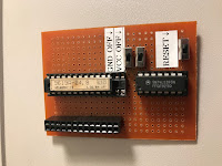
I soldered up a small carrier for the PAL and a binary counter IC to deal with the high address lines since I only have 8 output bits, and the PAL accepts 11 address lines (A5-A15). I also needed to add some switches to disable the PAL until the PIA is set up properly to avoid bus contention. Without that, the PAL gets hot! (Notice the brown burn mark on its paper label.) I wrote a BASIC program to run through all the possible address combinations for the PAL inputs, and list the PAL outputs, printing everything out in a nice layout. When an output from the PAL changes, the BASIC program adds a separator to the map and prompts for me to input the name of IC that the corresponding line is connected to.

Next, I had the program (not connected to hardware) run through the various addresses to the secondary decoder (U10) connected to the PAL to make a map of the I/O address space.

After paste-ing the files side-by-side on my Mac, here are the results:


                  MEMORY MAP                            I/O MAP
         |____________________________|          |____________________________|
0000:    |                            | FFC0:    |                            |
         |        > RAM               |          |        > U12 IRQ VECTOR    |
         |                            |          |____________________________|
         |                            | FFC4:    |                            |
         |_  _  _  _  _  _  _  _  _  _|          |        > U31 6821 PIA      |
         |                            |          |____________________________|
         |                            | FFC8:    |                            |
         |                            |          |        > U30 6821 PIA      |
         |                            |          |____________________________|
         |_  _  _  _  _  _  _  _  _  _| FFCC:    |                            |
         |                            |          |        > U29 6821 PIA      |
         |                            |          |____________________________|
         |                            | FFD0:    |                            |
         |                            |          |        > U27 6551 ACIA     |
         |_  _  _  _  _  _  _  _  _  _|          |____________________________|
         |                            | FFD4:    |                            |
         |                            |          |        > U26 6551 ACIA     |
         |                            |          |____________________________|
         |                            | FFD8:    |                            |
         |_  _  _  _  _  _  _  _  _  _|          |        > U28 6840 PTM      |
         |                            |          |____________________________|
         |                            | FFDC:    |                            |
         |                            |          |        > U28 6840 PTM      |
         |                            | FFDF:    |____________________________|
         |____________________________| 
A000:    |                            |               \                   /
         |        > U17 ROM           |                \_________________/
         |                            |                         |
         |                            |                         |
         |____________________________|                         |
C000:    |                            |                         |
         |        > U13 ROM           |                         |
         |                            |                         |
         |                            |                         |
         |____________________________|                         |
E000:    |                            |                         |
         |        > U7 ROM            |                         |
         |                            |                         |
         |                            |                         |
         |____________________________|                         |
FF80:    |                            |                         |
         |        > External I/O      |                         |
         |____________________________|                         |
FFC0:    |                            | \                       /
         |        > I/O               |  |_____________________/
         |____________________________| /
FFE0:    |                            | 
         |        > U7 ROM            | 
FFFF:    |____________________________| 

The map is upside-down due to how the counter IC increments, but still very helpful. Also, I'm not sure why the U20 socket isn't being addressed. It would make sense if it were in the $8000-$9FFF range though. Maybe a bad solder joint, or it is enabled by one of the other PAL connections that I was not sure how to simulate. Note that the $FFC0-$FFC3 range of the I/O decoder loops back to the PAL, which could then potentially enable something there.

PAL Mapper on the Apple //e PAL interface circuit board
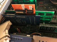
APIO card connected to PAL interface circuit board PAL Running in the Apple IIe