Showing posts with label 4164 DRAM. Show all posts

Monday, November 5, 2018

64K 4164 DRAM Decoding Integration

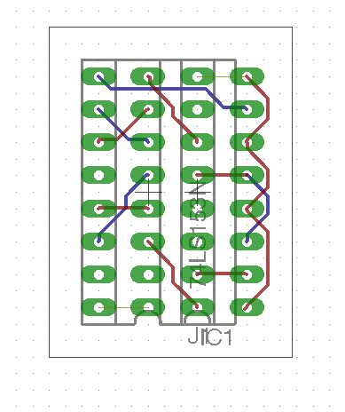
I integrated the 4164 DRAM decoder wiring into the logic board this weekend. It was very difficult to troubleshoot, and on retrospect, I think an adapter board would have been easier and less problematic. The main hangup was that the A14 signal to pin 10 of the J1 socket is connected on both sides of the logic board. One side in from expansion slot 7, and the other side goes out to H1 socket which creates the (A14&A15) signal. I had routed the (A14&A15) back to the J1 socket to decode the upper 16K of RAM. After disconnecting the A14 line from pin 10 and re-connecting pin 10 to a new video decoder signal (HIRES&PAGE2), the video decoder signal was getting sent through to H1 to give (HIRES&PAGE2&A15), which is wrong and caused computer to not be able to access the ROM.

Anyway, I fixed the problems and 74ls153 now sits in the J1 socket like it was always supposed to be there. The signals to decode the upper 16K of memory in the 4164 DRAMs are now available. I need to build circuit with registers to set to enable the upper bank and bank switch the 4K that overlaps the I/O area of the Apple II+. It will basically be 1/2 of an Apple 16K RAM/Language card.

Monday, November 7, 2016

RetroChallenge Epilogue and Apparent Success

After Review of my plan and schematics, I noticed a small error in the Eagle schematic I posted earlier.
  1. Pin 11 of the socket must be connected high (or to pin 12, or to a soft switch to enable video scanning on row E of RAM).
  2. Pin 11 of IC F2 must be disconnected and that line (not the IC pin) must be connected to ground instead (See my hand-drawn schematic).
I figured out problem 1 first. But when I booted I received half of a startup beep repeatedly, like it was stuck. It took a while until I realized I forgot Problem 2 since it was only on my older schematic. I used an IC socket and connected pin 11 and 12 and raised the IC leg. This is important as it decodes whether the Apple II is in RAM or I/O mode. The computer was stuck with no access to I/O or ROM (or simultaneous access to RAM and I/O or ROM).
F2 IC with pin 11 sticking out in a socket with pin 11, 12 connected It boots!

It seems to have worked! The computer shows the APPLE ][ greeting just as expected. I need to connect a keyboard and a disk controller card to test it all out and verify that all 48K is being accessed.

So, I now have an Apple II with 48K of 4164 DRAM in just one bank of RAM. Now for 64K. Or 128K...

2 banks of RAM installed for future 128K modifications


Tuesday, November 1, 2016

Final Push and Failure

I ran jumpers wires on the back of the Apple II+ logic board to route the various signals I needed (PHI_0, AX, A14&A15) to the J1 socket area. Fortunately since only half of J1 is used by the Apple II+, I can use the unused pins of that socket to route my signals through to the new circuit I am adding.

Here is my circuit diagram:

and the adapter board:

Warning - I don't know if this works yet.

After I ran the wires, I started trying to solder a tiny adapter board to translate the 74LS257 signal locations to the new 74LS153 IC. That was taking too much time for something that might not work at all, so I put the circuit on a bread board. Here it is:

Unfortunately, this did not work. I suspect that the dip jumper cable may be too long and adding some capacitance or delay. Or, the RAM timing may have been thrown off by the internal logic of the new IC. My Apple II+ is not booting and is in a similar state to when the RAM was in the wrong row. I'm sure I would have figured this out, but Halloween took priority.

Better news is that my Apple IIb is in a pretty final state. I think I will start buying supplies to actually build it.

Until next time, RetroChallenge!

Saturday, October 29, 2016

Apple II+ 64K RAM Refresh and Addressing

I managed to add my modifications back to the Apple II logic board to get the 4164 RAM enabled. It seems to be working! However, I want to address all 64K of the RAM, not just 16K. To do that, I need to refresh the extra RAM rows, multiplex the RAM row and column address for the new RAM address pin, and make sure that row C of RAM stays enabled instead of selecting row C, D, or E. See the detailed plan of attack by clicking below.

Friday, October 28, 2016

Troubleshooting Frustrations

I spent a number of hours last night and tonight trying to figure out why my modified Apple II+ was not beeping, and instead showing a screen full of question marks (or sometimes a white screen) on start-up, even after I added a row of 4264 DRAM. I swapped all of the ICs back and forth with my functioning Apple II+ and still had the same problem. At that point, I realized that I should have done some basic testing before I modified the logic board. I removed my modifications, and still had the same problem.

I found out that I could get very similar symptoms on my working Apple II+ if I removed the F2 74LS139 decoder, which selects which RAM bank to use. So I started checking continuity on my non-working board. I discovered that here wasn't continuity between the low bank selection line and the row that I had my RAM in. I thought I had found a major fault in the board. Then it hit me. The apple II+ rows are labeled A through K, and start with A on the bottom ROW. I had put my RAM in row E (the high address bank), instead of row C (the low address bank). I moved the RAM chips and after swapping out a bad chip, BEEP, and APPLE ][ at the top of the screen.

I felt so dumb. Hours wasted. So now I'm re-doing my modifications. Still time for some progress tonight. At least it's working. That logic board has't been fully functional in probably 30 years.

Tuesday, October 25, 2016

Apple II+ RAM Replacement - Power

Replacing the RAM in my Apple II+ has become a bit of a project in and of itself. Sure I could just buy some 4116 (16K bit) DRAM, but that's not very exciting, and its not an upgrade. So, Instead, I have been figuring out how I can use 4264 (64K bit) DRAM in its place. There are a lot of considerations that need to be made including power, refresh circuit, and addressing the new RAM. The descriptions below are for an RFI Revision 01 board, and may be different for other revisions. Click below to see the details of re-routing the RAM power lines and my preliminary results.