Wednesday, June 15, 2022

Synertek MBC020

I recently acquired a Synertek MBC020 EXORbus single board computer, notably sporting a 6512 microprocessor. The 6512 is software compatible with the famous MOS 6502 processor used in the Apple ][. This is one step closer to the whole point of this blog! It may at first seem odd that this 6512 board uses the EXORbus card edge which was most commonly associated with Motorola MC6800, MC6802, and MC6809 processors. However, the 6500 family was always intended to be MC6800 bus compatible. In fact, Rockwell even produced an AIM 65 Expansion Motherboard that would allow their AIM 65 computer (which like the Synertek SYM-1, was a derivitive of the famous MOS KIM-1 6502 trainer) to use EXORbus card modules. Synertek also made a clone of the MC6800 based Motorola MicroModule MM01, named the MBC01A2, and various EXORbus RAM and I/O cards.

Any of these ExorBus systems I have seen are either trainers or PLCs (programmable logic controllers) for industrial applications. They appear in knitting machines, industrial ovens, industrial food processing machines, and silicon wafer exposure and inspection stations. Fittingly, the Synertek MBC020 is usually seen configured for use in an "EG&G Torque Systems" servo controller. This is the same configuration for the card I purchased:
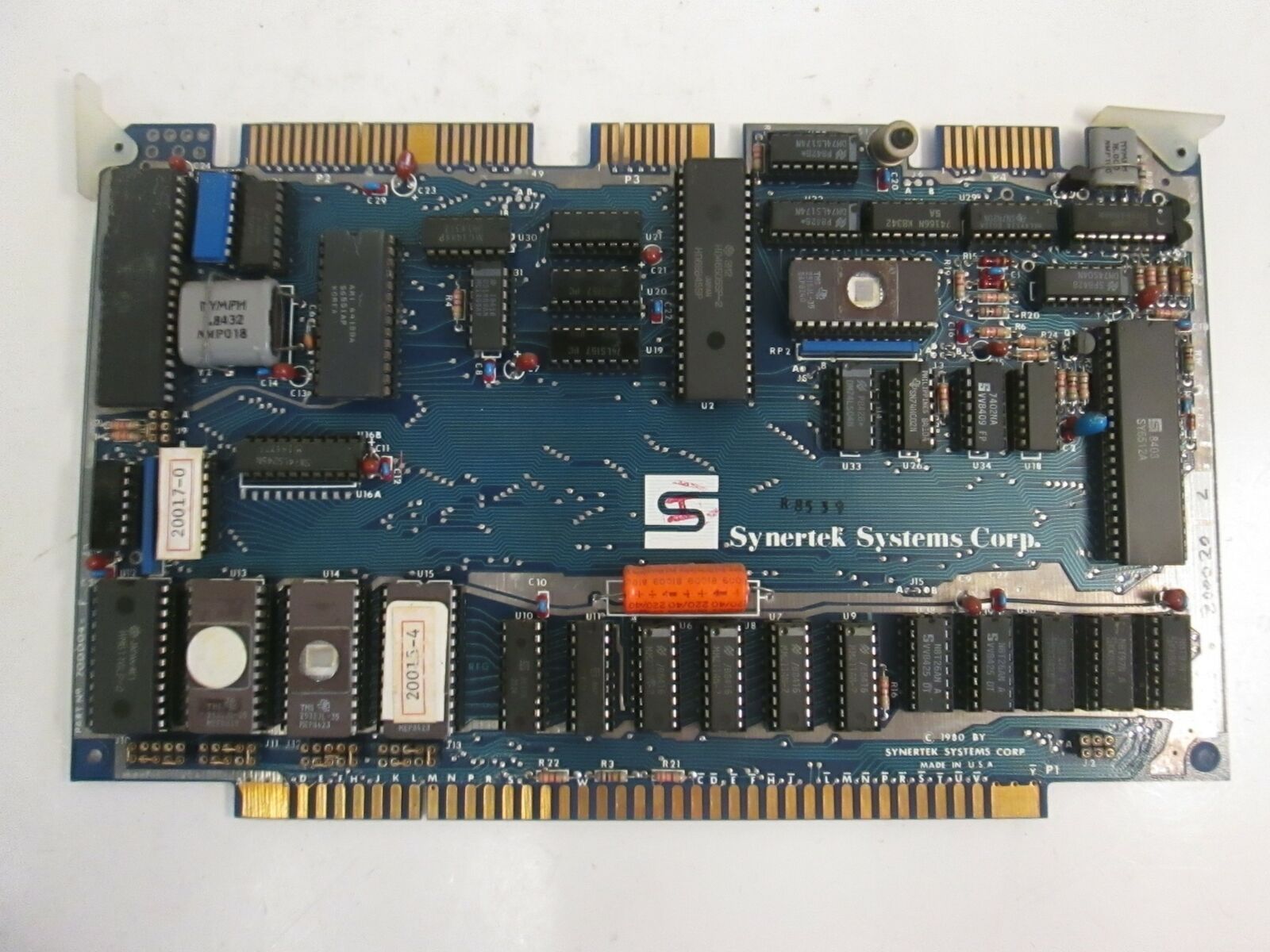
The Synertek MBC020 MOS 6512 based Single Board Computer

In a strange stroke of luck, this board happens to be available in the MAME emulator (formerly:"Multiple Arcade Machine Emulator"). I'm not sure why an industrial controller would be included in a emulator focused on arcade and console video games. Anyway, the ROMs available online appear to be the same as my own, so it is nice that I can see what I should be expecting when booting the board. Once I compiled MAME and added the ROMs, I was greeted with:

After a bit of trying out different key combinations, I discovered that the commands are predictably very similar to the SYM-1's SUPERMON monitor. Here is an incomplete summary:

SERVOMON COMMANDS: [] is optional parameter, $ is a hex digit (0-9,A-F)
Command and FormatDescription
M [[$$,]$$$$[-$$$$]]MEM: Memory examine, modify, [search,] hex data editor starting at address [-end]
R REG: Examine and modify user registers PC,S,F,A,X,Y
G [$$$$]GO: Restore all user registers [except PC=address, S=FD] and resume execution.
V [$$$$[-$$$$]]VER: View/Verify display data and checkums [starting at address [-to end]]
D [$$$$]DEP: Deposit hex data to memory [starting address]
C [$$,]$$$$[-$$$$]CALC: Calculate two's complement [-displacement], with [,offset]
B $$$$,$$$$-$$$$BMOV: Move data to address, from start -to end
J $JUMP: Restore user registers, except PC=listed entry in jump table, S=FD, and jump to it
J 1 MPC DIGITAL DRIVE REV 4.0 JUL-1983.
AXES FOUND ONLINE : 1
Ok
SD $$$$-$$$$SDBL: Store double byte from address -to address
F $$,$$$$-$$$$FILL: Fill data, from memory address -to address
S1 [$$$$]Save ASCII data to memory [starting address].

Next post: let's try out the real board!

Sunday, June 5, 2022

MIKUL 1MiB Mods (final)

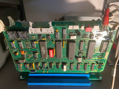
It did not take long for me to realize that the virtual address jumper board for my MIKUL 6218 was not a great long-term soloution. It was ugly and was not very physically secure with jumper wires running everywhere. Instead, I decided to remove the jumper board and add a 2*5 pin header to the top of the memory board, where it belonged. As a result, I would need to program a GAL to go back in place of the jumper board, handling the conversion from virtual to physical addresses. Since I now have a working GAL programming pipeline, this was no longer a serious impediment.

Header

Adding the pin header was a simple matter of drilling holes in the board in a .10" grid, supergluing a 2*5 male header (with latch) to the board, adding some copper tape connected to ground, and soldering on jumper wires connecting to the A16-A20 address lines. Although I would have preferred to use some mounting screws on the header, both of the mounting holes ended up right on top of VCC traces.

GAL Program

With the board soldered up, I had some initial success using it with my CMS 9639 and Microware OS9 Level 2. However, I soon noticed that there was a block of memory that was not being identified at $C000-$DFFF every 64K. This is an odd range of addresses to have a problem with, since it can't be attributed to bad connections on an address line or two. I quickly identified that the GAL in U10 will disable the RAM and enable the I/O in that range, regardless of the state of the high virtual address lines. Although this is fine for the MIKUL 6809-5 board it was designed for, it is not consistent with the CMS9639's expectation that I/O is only enabled in the $00FF60-$00FF9F address range. So, I had to reprogram the U10 GAL and make some adjustments to the program in the U13 GAL to get everything working properly.

Conclusion

Here is the final product, a relatively clean looking 1 MiB EXORBus RAM and 3xVIA I/O card working great with the CMS 9619 and OS9 Level 2 on the CMS 9639:

Sunday, March 27, 2022

MIKUL 6809-5 Keypad

I received some membrane keypads in the mail today. Unfortunately, I neglected to order the 4x5 Keypads I hoped to use and only ordered 4x4 and (accidentally) 3x4 keypads. No problem. The 4x4 keypad will work fine to navigate the menus, with: * as clear; # as enter; D as Main Menu. You can't quite set the clock though because it is missing the keys to select year/month/day as they are on the missing row.

Here is the pinout, which requires a small jumper board to connect to either a 4x4 or 5x4 keypad, as the P3 header is not arranged in a very logical way:

  MIKUL 6809-5        eBay    |   Alltronics
   P3 HEADER       4x4 Keypad |   5x4 Keypad
        ___ 
COL1   |1     ->   3 - ROW3   |   6 - ROW3
ROW1  ||2     ->   5 - COL1   |   5 - COL3
COL2  ||3     ->   2 - ROW2   |   2 - ROW2				
ROW2  ||4     ->   6 - COL2   |   7 - COL4
ROW3  ||5     ->   7 - COL3   |   9 - COL5
ROW4  ||6     ->   x - N/C    |   3 - COL2
COL3  ||7     ->   1 - ROW1   |   8 - ROW1
ROW5  ||8     ->   8 - COL4   |   1 - COL1
COL4   |9     ->   4 - ROW4   |   4 - ROW4
       |___      

I think these are the orignial keypads that came with the TEMPMATE and CASEMATE firmware (pics from various auction sites):

Unfortunately, I think the cheap ebay 4x5 keypads I hoped to use will not work because they have 5 rows when the MIKUL's TEMPMATE software is written to use a keypad with 5 columns.

I found a keypad at Alltronics that has the right layout for only a few dollars. That keypad only has the flat flexible cable without a PCB connector, so I had to source that too. Also, it does not have the nice clicky metal domes in it so it feels mushy, but it works, and I can finally set the clock!:

Saturday, March 19, 2022

MIKUL 6809-5 Memory Map

By using the HCF instruction and a cheap logic analyzer, I was able to make a memory map of the MIKUL 6809-5:


External
 
FFFF


MEMORY OR I/O

EC00
EXTERNAL I/0 EBFF
EB10
U21 6821 PIA EB00-EB0F
EXTERNAL I/0 EAFF
EA10
U20 SIO/2 EA00-EA0F
U25 VRAM

MEMORY?
E9FF


E800

External
E7FF


MEMORY


0000

Of course, this lines up well with the MIKUL 6218 memory and VIA board. I need to update that memory map using the HCF technique.

Reverse Engineering MC6809 SBC... The Easy Way!

I previously documented my ultimately successful attempt to reverse engineer the CMS 9619 Advanced Single Board Computer. The main goal was to get a memory map of the system, including I/O addresses. Having this memory map makes disassembling the firmware on these boards much easier. The process I used prevously was labor intensive, and required me to:

  1. figure out what each of the pins on the PAL IC (that decodes the addresses) connects to;
  2. lookup datasheets to see if it is an input or output pin;
  3. build a small circuit to increment through all of the possible inputs;
  4. write a program to display all of the actual outputs for those inputs.
This took a lot of work and most of it is will only apply to the particular address decoder I was working on.

Ideally, I would want to just keep everything connected in circuit and just have the processor increment through all of the address lines for me, like a 16 bit binary counter. Hmm... Fortunately, the MC6809 has just such a feature built in! The "HCF" (Halt and Catch Fire!) instruction will halt the processor and increment the MC6809 address lines while holding R/W' high, causing it to output every possible address, and select every I/O chip on the board. This is perfect to build a memory map. Even better, since just one instruction does all of this, all I need to do is wire up that one instruction on the data bus and let the processor do the rest. I don't even need to program an EEPROM! Then, I can just observe the addresses and I/O enable lines using a cheap (under $10) logic analyzer. I could even use an Apple II (or another 6809 SBC) with a MC6821 PIA (or MC6522 VIA) to track the signal changes.

In the end, I decided to just program an EEPROM with a lot of HCF instructions: % touch HCF.bin % os9 padrom -c=205 8192 ./HCF.bin % minipro -p AT28C64 -w ./HCF.bin % xxd -s $((16#1FF0)) ./HCF.bin

00001ff0: cdcd cdcd cdcd cdcd cdcd cdcd cdcd cdcd
and I used my cheap logic analyzer to check the addresses and the chip select pins on the various I/O ICs on the board. Although this took a couple of steps (A15-A9 addresses, then A8-A2 addresses, before settling on A11-A8 with 4 chip select lines), I think it was probably faster than building a cable to connect to the Apple II APIO (MC6821) card, and I am pretty sure the Apple II could not have polled the lines fast enough.
Note channels 3-7 (A11-A7)incrementing nicely with HCF instruction

Wednesday, March 16, 2022

MIKUL 6809-5 Processor and Video Board

I recently procured another EXORbus processor board, the MIKUL 6809-5, for a reasonable price. Let's take a look...

Notable ICs:

  • Motorola MC6809 processor
  • MC6821 Peripheral Interface Adapter (PIA)
  • MC6847 Video Display Generator (VDG)
  • Z0844206 SERIAL INPUT/OUTPUT CONTROLLER (SIO/2)
  • MM74C923 20 Key Keyboard Encoder

Ports:

  1. EXORbus card edge
  2. RS232 and RS485 / multidrop LAN port?
  3. 20 key matrix keypad
  4. LED indicator ?
  5. video output
  6. composite video

It is interesting that the board uses the MC6809 CPU with a MC6847 VDG like the Radio Shack Color Computer (CoCo). Unike the CoCo, it does not have an MC6883 SAM, making it similar to the Radio Shack TRS-80 MC-10 (which uses an MC6803, rather than the MC6809). So the basic CPU and video chipset places it somewhere between those two computers.

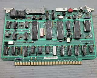
Notably, the board does not have any provision for ROM or application RAM on it. As a result, it needs another memory board on the bus to function properly. The MIKUL 6218 would make a perfect companion for it, but I already modified my 6218 board to work with the my CMS processor boards...whoops. So, with the price of these MIKUL boards dropping due to an apparent glut of them, I picked up a fresh MIKUL 6218 for ~$35 and installed them both in my EXORbus MULTI-PLANE backplane.

Despite the interesting video output, I am not in love with the features. The MC6821 PIA is dedicated to running the keypad encoder and baud rate dip switches, so it can't be used for much. Really the MIKUL 6809-4 or 6809-6 (Motorola MicroModule clone?) would be a better choice as a all-in-one SBC. However, the 6809-5s are definitely more pentiful and far cheaper right now, so maybe somebody else can make use of any info I publish about it.

More details below...

Sunday, October 31, 2021

RC2021/10 Final post

Well, I ended up having a very busy October (baby is due November 1st!), so I didnt get much done for RetroChallenge. I kept looking for a Zaurus I/O connector or serial cable on eBay, but did not have any luck. That said, I feel good that I helped organize my first RetroChallenge event, and I think it was a great success with 44 entries! I also did some programming on Google Suite to set up some infrastructure for the event. So, all in all a good month, despite the lack of retro computing!

Sunday, October 17, 2021

Stylus Fix

Well, with virtually no hope of getting a serial cable for my Zaurus, I moved on to some other bits that the Z needs. Really soon after I bought this thing, I managed to drop the stylus and break the tip off. I tried super glue in the past but it would not hold for very long. When I pulled it out of the box, it saw that I had wrapped electrical tape wrapped around (all gross and sticky after 5+ years) it and could not fit in the handy stylus holder built into the body of the Zaurus. Oh, the indignity! First I had to get the broken threaded base out of the body of the stylus. Since it had broken off flush with the body, I could not grip it. I had to use a small file to cut a channel in the plastic to fit a flat head screwdriver. Then I was able to unscrew it from the metal.

I have had good luck lately using ABS glue on all sorts of automotive plastic, so I thought this guy would be a good candidate.

After applying some of the ABS cement (typically used for septic pipes), it was clear that the plastic was getting gooey and would make a nice chemical bond. I put the stylus in a framing square to keep it straight, and I now have a nice usable stylus for my useless Zaurus!

Not much progress, but it's something!

Friday, October 1, 2021

Early Roadblock

About the Sharp Zaurus SL-5500

Before I begin with details on my project, here is some background on the Sharp Zaurus, as it was relatively unique, but quickly got lost in a sea of newly released PDAs during the early 2000s. It was unusual in that it ran a linux kernel from the factory and gained a cult following with techie types and hackers. Some promotional material:
Zaurus brochure front
Zaurus brochure back
See the PDF Version of this brochure

Getting the Zaurus running

Getting my Zaurus working again was a simple task. I thought for sure that it would need a new battery, but after charging it for a few hours today, it seems to be running and holding a charge. It did not work at first, but I took out the battery to take a look at it, and it started right up once I put the battery back in. I forgot that removing the battery resets it to the factory flash image. I don't know how long the battery will stay charged, but it seems like enough to get this project working.

Starting my Project

Unfortunately, finding a cable to fit my Zaurus IO port is proving to be quite difficult. I recall buying a cheap usb charging cable for it back when I bought it with the intent of making an RS232 adapter. Now, I can't find the cable and I am pretty sure I tossed it out a few years ago when I sorted through my boxes of USB cords. I thought I found the cable for sale online and proceeded to impulse-buy $50 worth of Zaurus accessories, but two weeks later I still don't have a response to my emails or a package from them.

It was a mistake to think this online store had
cornered the market in new old stock Zaurus accessories

I see many online stores with the official Sharp CE-170TS RS232 cable on sale for about $5.00 (unreasonably cheap), but those sites look even less legitimate than the store I bought from and all seem related to the same scam/owner. There are some cables on auctions.yahoo.co.jp that look like they would work, but I have never bid on there, would probably need a broker, and I have no idea how long it would take to arrive. I can't even find just the connector for sale by its part number. So, I am kind of stuck.

If I can't find a solution to this problem very soon, I am going to have to move on to other projects. I welcome any suggestions for finding this cable or connector.

Thursday, September 9, 2021

First Post for my RC2021/10 Entry

Well, I had hoped to do some work on an Apple II project, but my theme category for RC2021/10 "The Millennials" isn't getting many particpants. As a result, I will join the fun there and work on my circa 2002 Sharp Zaurus SL-5500 linux based PDA, hopefully completing a ridiculous project that I always wanted to do.
To do List:
Dig the Zaurus out of my "Sell on eBay" bin.
Replace the battery (it only lasted 1/2 hour to begin with)
Install a mouse driver
Get a serial mouse connected and working
End goal: Use the Zaurus, directly mounted on the mouse, as video display/keyboard/mouse to interact with VNC running on the Zaurus to control my Mac.

Wednesday, June 16, 2021

CMS 9619 Address Decoder Replacement

In my previous post on the MIKUL 6218 board, I mentioned that was using the lower 32K of address space on the CMS 9619 to swap in 16 banks of external RAM. You may remember that I had previously made some minor modifications on the CMS 9619 to use this space for an on-board 32K SRAM chip and still use the external I/O. What is happening here? Well, I had to remove all of my wire modifications to the CMS 9619, and restore it to the standard arrangement. With my new GAL programmer in hand, I figured out the logic equations to replicate the CMS 9619's U12 address decoder. I made an adjustment to how the U20 ROM/RAM socket and bus tranceiver are addressed so that I can have one GAL to have all 64K on-board and another for the standard external 32K. Now I can just swap out the GAL ICs to change the arrangement!

GAL and ROM options

There is still a small glitch in UTIL_DECODE that I have to resolve (I think this is why CMS orginally used XOR logic PAL20L10 rather than the more common NAND logic PAL20V10), but everything seems to work great.

If you need a replacement decoder for your CMS 9619, or just want to make some modifications to the memory map, this is the way to do it!

MIKUL 1MiB Mods (continued)

With the virtual address jumper for the MIKUL 6218 sorted, I still needed to simplify the address decoding and memory chip selects so that 1 of the 4 SRAM sockets will be selected depending on the state of our virtual A19 and A20 addresses. Since the three I/O ICs (6522 VIAs) share the data bus with the memory, I also need to disable the memory when the I/O is active, and signal the GAL in U10 to select the appropriate 6522 VIA.

Fortunately, the CMS 9619 and 9639 use several signals (VMA, VUA, or UTIL_DECODE) to indicate when the processor board is addressing external memory or I/O. This greatly simplifies the decoding from the original MIKUL arrangment which had the GAL fully decoding all of the address lines from A6 through A15. But, since the MIKUL 6218 board does not use those CMS/EXORbus decode signals, I had to cut a few of the unneeded low address lines to the GAL and replace them. With this simplified arrangement, I had hoped to use a few standard 74LS logic ICs to select the RAM and I/O. But, after a few attempts reduce the number of logic chips I needed, I decided to bite the bullet and just get a GAL programmer.

Here is my new setup which seems to work great with macOS:

  • XGecu TL866II plus USB programmer - programs the GAL
  • minipro - reads and writes JDEC files to the TL866
  • GALasm - turns logic equations into JEDEC file
The biggest obstacle was that the first programmer I ordered (an older model TL866A) did not work due to a faulty pin 10. Unfortunately, this has been my luck with new tech items from China, including the cheap logic analyzer I bought a while back. These kinds of issues take A LOT of time to figure out.

Once I received a functioning programmer, I managed to get everything working well with my CMS 9619. So, now I can switch in 16 blocks of 32K RAM (512K) into the lower half of the CMS9619 address map, using the low nibble of its PIA output (at $FFC4) as a register to drive the virtual address lines. The CMS 9619 does not output a signal on its PIA for A20, so I can only use 2 of the SRAMs. Also, since the RAM addresses overlap the CPU addresses, half of each 512K SRAM chip can't be accessed (when A15 is high). This could be easily fixed by modifiying the U13 jumper board that I made previously, or even the CMS 9619 address decoder. Honestly, the original configuration was probably better for the CMS 9619 because it did not switch out the lower 8K of RAM that an OS would use. However, since my end goal is to use this with the CMS 9639 CPU and its integrated MMU, I will keep it as-is. I haven't fully tested the I/O and the VIAs yet, but I will get to those soon enough.

512K RAM on a MC6809!
Note the rainbow virtual address jumper and the
additional jumpers to route A19 and A20

More of the techincal details below, after the break...

Wednesday, April 21, 2021

MIKUL 1MiB Mods

A18 Addition

I really want to use my two 512KiB SRAM chips on this board to maximize the usable RAM. Fortunately, the MIKUL 6218 has 32 pin DIP sockets, so my SRAM physically fits. However, pin 1 (A18) of the socket is connected to VCC, limiting each socket to 256KiB (2^18) of memory. This is strange because four 256KiB (2MBit) SRAM chips would be perfect for this board (and my needs) but are quite unusual and are actually more expensive than four 512KiB (4MBit) SRAM chips.

To increase the socket capacity to 512KiB, the trace connecting A18 to VCC for each memory chip must be cut. Unfortunately, this is a wide power trace that is hidden under the end of the sockets. A few seconds with an 1/8" drill at a 45° angle cut through the A18 pull-up trace without too much collateral damage. Although I slightly cut into the socket, I barely avoided cutting into the next thin address line down.  

A18 to VCC severed.

Then, I added a few wire jumpers to connect pin 1 of each socket to each other to give a common A18 line. This address line, along with A16 and A17, need to be connected to a new virtual address header. A19 and A20 will be connected from this header to a decoder to create the memory chip select signals.

Bank Address Eliminator

With the physical connections made, it's time to simplify the MIKUL 6218's memory bank select system.

This little jumper board just connects each real address to its respective memory address line (A11-A15), overriding the bank switching latch and logic at U13. The virtual addresses (A16-A20) connect to the 10 pin header which will connect to the main CMS 9639 processor board. The 3 pin header on the right will connect A19 and A20 to a decoder to select the correct memory chip.

With the RAM and this board in place and the virtual address lines pulled high, the board works exactly the same way as it did before and has the same memory map. However, the bank register functionality (which I could not test anyway) has been eliminated. But, without the virtual addresses, I can only access some of the RAM.

Next time ... the RAM chip select Decoder

Tuesday, February 2, 2021

CMS 9600A MPU Revival

I was recently able to trade one of my extra CMS 9619 SBCs for a CMS 9600A MPU (Thanks Joel!). This EXORbus processor card has very similar specs and layout to the CMS 9609 MPU card, but it uses the Motorola 6802 processor (an MC6800 with integrated RAM), rather than the MC6809.

If you are ambitious enough, you could even modify the CMS 9600A to use a MC6809 processor. Neither of these boards are as advanced as the CMS 9619 single board computer I have been working on, but nonetheless, I have been eager to get my hands on a MC6800 system to play with.

The board is in great condition, but had some areas of concern:

  1. There are no RS232 line drivers installed, instead using DIP program headers/shunts in their place.
  2. There is no boot or debugger ROM installed.

I mostly addressed the second concern before I even received the board. I OCR'd and transcribed the SYSMON debugger from the source code in the CMS 9600 manual (thanks for the scan Roland!). With a few adjustments, I was able to assemble it and format it for programing to EEPROM. Unfortunately, I could not get my AT26C16 EEPROMs to program in-circuit as I have for the AT28C64 EEPROMs. Anyway, I ended up using an adapter to use 1/4 of an AT28C64 EEPROM for testing.

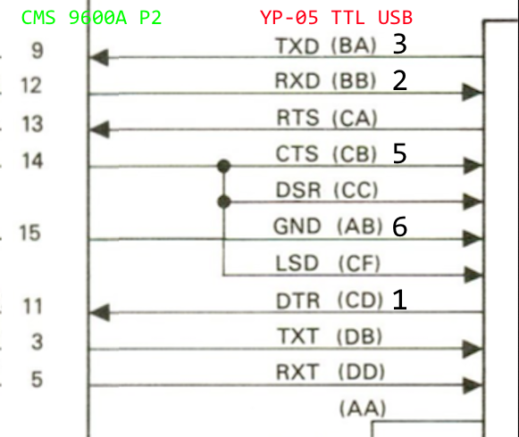
As for the missing RS232 line drivers, this board was configured to use external line drivers on an RS232 breakout module (likely the CMS 9601-501). I tried connecting the appropriate serial lines directly to a TTL to USB serial adapter, but I did not receive any response from the board. I decided to just buy and install the line drivers to be consistent with my other CMS boards. This would eliminate a few variables while I focused on getting everything to boot from the EEPROM. Once I installed them it became clear that the new drivers were interferring with the baud rate generator due to an unusual wired jumper configuration that was causing contention. I removed some of the wire wrap jumpers so the settings are more consistent with my CMS 9609 board, and observed a nice clock signal arriving to the ACIAs.

Next, I added a small jumper to bring a constant 12V to the Power Failure Protect/Restart Circuit (connect 12V VIA to the "CR2" through-hole). Without it, the board stays in "locked reset" due to an assumed power failure.

While I was debugging these issues, I noticed a few distinct puffs of white smoke coming out of the CPU! I am not sure how that happened. I assume one of the address lines was pulled to ground through a test lead, but I was being quite careful. Anyway, with the CPU shot, I had to wait a few weeks for a replacement to arrive.

With a new CPU installed I was still troubleshooting with the logic analyzer when I noticed a column of asterisks in the terminal! I double checked the manual and realized that the monitor had been prompting me for a command for several reboots!

*V
FROM ADDR FF80

FF80 04 48 49 4E  5A 56 43 0D  0A 15 00 04  0D 0A 42 4B  
     .HINZVC.......BK
FF90 41 44 44 20  04 0D 0A 46  52 4F 4D 20  41 44 44 52  
     ADD ...FROM ADDR
FFA0 20 04 0D 0A  54 48 52 55  20 41 44 44  52 20 04 54  
      ...THRU ADDR .T
FFB0 4F 20 41 44  44 52 20 04  56 41 4C 55  45 20 04 4D  
     O ADDR .VALUE .M
FFC0 FA 42 45 F8  9B 47 F9 14  52 F9 35 54  FA A2 48 F9  
     .BE..G..R.5T..H.
FFD0 B7 56 FD DD  49 FA 07 4A  F9 FD 46 FA  67 51 F8 1C  
     .V..I..J..F..Q..
FFE0 44 FA 9D 4B  FA B4 31 F9  00 32 F8 EF  4C F8 1C 53  
     D..K..1..2..L..S
FFF0 F8 1C 4F F9  B6 4E F9 B8  F8 4F F8 59  F8 54 F8 00  
     ..O..N...O.Y.T..

Once I knew that everything was working, I took another stab at programming the EEPROMs in-circuit. After some jumper configuration changes on my CMS 9619A, I was finally able to program a few 28C16 EEPROMs. As it turns out, the CMS 9609 has some timing differences from the CMS 9619 that apparently prevent it from programming the EEPROMs. But with the CMS 9619 configured to accept the smaller 24 pin 28C16 EEPROM, the programming worked fine.

With everything else up and running, I wanted to try a TTL level USB/serial connection using the board's original DIP program headers, rather than the RS232 drivers that I added. Following the manual, it was easy to swap out the drivers and connect it up:

PHEW!

Sunday, January 3, 2021

MIKUL 6218 Memory and VIA EXORbus board

I haven't spent much time working on my CMS 9639 SBC because, unlike the CMS 9619, it does not have any usable on-board RAM and does not include a monitor/debugger in ROM. Instead, it is designed to use an external memory board (which I don't have) on a back plane (which I now have) and boot OS-9 from a disk drive (which I don't have). What is nice about the device is the built-in memory manager which uses up to 1MiB of RAM. Unfortunately, EXORbus RAM cards are still prohibitively expensive on eBay and only have 16K to 64K of RAM capacity. Since the components would be far less than the price of those boards, I took a stab at designing a 1MiB SRAM board with a bonus additional I/O expansion.

I had just started to get components inserted into an EXORbus prototype board when I noticed the MIKUL 6218 Memory and VIA boards appearing on eBay at reasonable prices (<$45 shipped). Let's take a look at the board:

Click below for more details...

Wednesday, December 16, 2020

NitrOS-9 boot from ROM

One of the shortcomings of this CMS 9619 system is the fairly complicated OS9 bootstrap procedure I had to use in the absence of any sort of disk drives. To summarize:

  1. DEBUG19 (in ROM) starts
  2. Host computer transfers a small loader program using DEBUG19's memory edit routine
  3. DEBUG19 jumps to the loader program, loading the kernel track from the drivewire server and runs it
  4. NitrOS-9 starts and continues loading the rest of the bootfile from drivewire
This works pretty well, but has several drawbacks:
  • 8K of address space is taken up by DEBUG09 ROM
  • The host computer needs a separate script to efficiently transfer the loader program using DEBUG19
  • 2 x 256 byte blocks of RAM need to be reserved to hold the RAM interrrupt vectors and data for DEBUG19

I had hoped that the kernel file could run from ROM and directly load disk images from drivewire. Unfortunately, the NitrOS-9 code is tied closely to the CoCo's hardware, and always relocates the kernel from ROM to RAM. To combat this problem, I replaced NitrOS‑9's relocation routines and added a module to initialize the CMS 9619 hardware for booting directly into the NitrOS-9 kernel. From there, the NitrOS-9 booter (on ROM) will load a disk image over drivewire. This is very similar to the set-up for the CMS 9639 (and I assume other computers sold with OS9). NITROS9 ROM BOOT NitrOS-9/6809 Level 1 V3.3.0 CMS 9619A (C) 2014 The NitrOS-9 Project ** DEVELOPMENT BUILD ** ** NOT FOR DISTRIBUTION! ** Wed Dec 16 16:07:07 2020 http://www.nitros9.org * Welcome to NitrOS-9 Level 1 * * on the CMS 9619A ASBM * yyyy/mm/dd hh:mm:ss Time ? 2020/12/12 05:55:55 >> Clock Initialization Errors << December 12, 2020 05:55:55 Shell OS9:

(The Clock init Error is because the code currently expects the DEBUG19 clock setting routines to be installed in ROM, which they are not. I still need to add these.)

It took some careful configuration to ensure that the CMS 9619 can boot from the DEBUG19 loading process OR directly from ROM, with no wasted memory in either case. Since the final NitrOS-9 boot ROM is less than 4K in size, an abbreviated DEBUG19 can also be programmed into the EEPROM. The code is available on Github.

On the note of programming EEPROMs, I discovered back when I was disassembling DEBUG19 that I can use DEBUG19's memory edit routine to program an EEPROM on the board. Of course, the timing is all wrong and the editor returns an error because the EEPROM takes much longer to store the value than RAM would. With some help from an expect script, it is fairly easy (though slow) to continuously run the memory edit routine, once for each byte, and ignore the errors. So, I can program EEPROMs on board by simply moving a jumper and running the script. If anybody has one of these boards without a ROM, I would be happy to send you a fully programmed EEPROM with NitrOS-9 and DEBUG19. In fact, I think I will add that to my tindie store soon!

Friday, October 23, 2020

Never Valid User Address

After finding out that my CMS 9619 Advanced Single Board MicroComputer was having problems accessing the EXORbus, I tried some trouble shooting. My MULTI-PLANE EXORbus backplane made it easy to accesss the various signals with an extra card edge receptacle attached. I tried pulling down various lines of the data bus with a resistor, and noticed that the 8 bits of data seemed to be responding appropriately. So, probably not the data bus tranceiver.

With little more to go on, I ended up buying an inexpensive USB logic analyzer and installing PulseView software for it. I was quickly able to identify that the bus's VUA (Valid User Address) signal was not rising when it was supposed to, even though it was receiving the correct signal from the PAL address decoder. Without this signal, the I/O card was never properly addressed, and the data bus was always floating. I tested another CMS 9619A board I have which displayed similar symptoms and found that it too was suffering from a failure of the same IC. Odd coincidence. So, after some desoldering, super-gluing a trace that was inadvertently partially pulled off the board, and re-soldering a new 74LS244 8-bit driver (U9), I am back in business. The chip came off of the other board much easier with the help of a heat gun.

I can't recommend these cheap logic analyzers enough to a hobbyist, although the first one I recevied was not working properly on some channels (make sure to test them before you rely on them for anything).

I also bought an EspoTek Labrador USB oscilloscope to try out, but I received, tested, replaced, and finally used the cheap logic analyzers from ebay while I was still waiting for the Labrador to arrive.

Thursday, October 8, 2020

CMS 9619 Hardware Mods (continued)

Update: Since this post I have figured out how to change the address map using a GAL IC.

I recently posted some minor hardware modifications I made to my CMS 9619A Advanced Single Board Microcomputer to get it to use a 32K SRAM chip. Unfortunately, I had to disable the EXORbus data bus transciever to get it to work. So, although the board works properly as a single board computer, it cannot access the EXORbus. With NitrOS-9 up and running, I would really like to regain the ability to use external I/O cards.

To get this to work, the data bus transceiver (U11) needs to be re-enabled, but only during the External I/O address space at $FF80 to $FFBF (checkout the CMS 9619 memory map for details). This can be done by combining the normal data bus transceiver enable signal with the signal for address line A15. This works because the only time the transceiver is normally enabled in the high address space is in the External I/O address space (because everything else in that range is onboard the CPU module). All we should need to do is invert the normal data bus transceiver (U11) enable signal, and NAND it to the A15 address line.

Fortunately, there are a few ICs on the board that are not fully utilized. We can use the 1st gate (pins 1->2) on the U1 74LS04 inverter IC to invert the data bus transceiver enable signal, and the first gate (pins 1+2->3) on the U3 74LS00 gate IC to NAND the inverted signal to A15.

 
No traces visible to pins 1 or 2 on U1 or U3

This is almost too perfect that these logic gates are available, so I'm sure it won't work. Also, since the board is already bodged in this area with the factory's dead-bug'ed delay line, all of the modifcations are easily reversible with no traces to cut.

Before Modifications Schematic
Before
After Modifications Schematic
After

After the modifcations, everything booted up properly and I was able to access my 32K SRAM at $0000-$7FFF However, I was unable to read any data from my known-good CMS 9650 8 port Serial I/O card. After some basic troubleshooting, I got to thinking... I don't think this processor card was EVER able to access the external bus- which is why I think I chose it for modfications. Major troubleshooting to come...

Wednesday, September 30, 2020

CMS 9619 Drivewire Boot to NitrOS-9

I finally got drivewire running on the CMS 9619 SBC. As a result, I managed to complete the bootup and have a virtual disk! Source code available on github.