 |
| Note the 5 28 pin sockets on the right side of the board for 4K or 8K SRAM or ROMs |
In order to get NitrOS-9 running on my CMS 9619 SBC, I am going to need a lot more RAM. This board is configured to have up to 8K of onboard RAM and 32K of onboard EPROM, with options to use 4K or 8K chips. 32K and 64K RAM expansion boards were available in several configurations, including battery powered non-volatile SRAM to retain state during power off. Unfortunately I haven’t seen any of these available at a decent price, so expansion boards are not a good option for me. I do have a 32K SRAM chip with a similar pin-out (part of an eBay Dragon 32 IC kit) to the 8K module which would fit nicely.
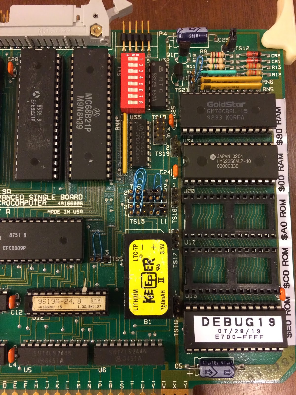
My board already has 8K of RAM installed in socket U34 ($8000-$9FFF), and 8K of ROM in socket U7 ($E000-$FFFF). Socket U20 is not selected by the PAL decoder on this particular board, either by design (being configured for 1 x 8K DIP SRAM vs. 2 x 4K SRAM) or due to some problem with the PAL. My new 32K SRAM needs to be selected and addressed, which requires some minor modifications to the board.
To select the new 32K RAM chip, I first raised pin 16 of the PAL decoder IC normally responsible for enabling the U20 RAM socket (apparently not working on my board). Once that was done, I used the A15 address signal to enable U20 socket instead. This required a short jumper wire from pin 3 (A15) to pin 16 (U20 CS') across the PAL address decoder. So now, whenever the A15 line is low ($0000-$7FFF), the SRAM in U20 will be enabled. This is perfect since the SRAM IC is 32K, and will fill the bottom half of the board's address space.
To address all 32K of the SRAM, I first cut the GND signal from pin 1 of the U20 socket. This is tricky since the trace is right against the socket. I ran a jumper from pin 5 of the PAL decoder to pin 1 of the U20 socket (A14). Then I set the jumper at TS19 to connect pins 2 and 3 (A13), and the jumper at TS6 to connect 8 and 10 (A11). Socket U20 now has the address lines it needs to decode all 32K of memory.
 |
| Two long jumpers to connect A13 (I realized later this is handled by jumper TS19) and A14, and one short jumper for A15 |
I was hopeful that everything would just work with the modifications, but of course it wasn’t that easy. The problem has to do with the data bus transceiver (U11) on the board. It is driving “data” from the EXORbus onto the processor data bus in the address range of the new RAM. However, there isn’t anything on the bus to drive and it is just causing contention with the new SRAM. For now, I disabled the transceiver by disconnecting the dead-bug'ed delay line from the enable pin (pin 19) of the transceiver, and pulled that enable pin high with a short jumper wire to Vcc. This isn’t ideal because it disables all of the external bus, including the I/O address range in addition to the low memory range that we need. So right now the CMS 9619 can’t read anything else on the EXORbus.
 |
| Short jumper to disable the EXORbus data bus transceiver (U11) |
So, with 40K of RAM (8K in U and 32K in U20), and 8K of ROM with sockets for another another 16K, the board is nicely outfitted to run some real programs.
OS-9 can run from ROM, so you should be able to put the OS modules in EPROMs, leaving more RAM for programs. Really enjoying this series.
ReplyDeleteYes, I tried that but I didn't have all the bugs worked out yet. Much easer to make changes to the RAM until I have a solid build.
Delete