Showing posts with label MIKUL. Show all posts

Sunday, June 5, 2022

MIKUL 1MiB Mods (final)

It did not take long for me to realize that the virtual address jumper board for my MIKUL 6218 was not a great long-term soloution. It was ugly and was not very physically secure with jumper wires running everywhere. Instead, I decided to remove the jumper board and add a 2*5 pin header to the top of the memory board, where it belonged. As a result, I would need to program a GAL to go back in place of the jumper board, handling the conversion from virtual to physical addresses. Since I now have a working GAL programming pipeline, this was no longer a serious impediment.

Header

Adding the pin header was a simple matter of drilling holes in the board in a .10" grid, supergluing a 2*5 male header (with latch) to the board, adding some copper tape connected to ground, and soldering on jumper wires connecting to the A16-A20 address lines. Although I would have preferred to use some mounting screws on the header, both of the mounting holes ended up right on top of VCC traces.

GAL Program

With the board soldered up, I had some initial success using it with my CMS 9639 and Microware OS9 Level 2. However, I soon noticed that there was a block of memory that was not being identified at $C000-$DFFF every 64K. This is an odd range of addresses to have a problem with, since it can't be attributed to bad connections on an address line or two. I quickly identified that the GAL in U10 will disable the RAM and enable the I/O in that range, regardless of the state of the high virtual address lines. Although this is fine for the MIKUL 6809-5 board it was designed for, it is not consistent with the CMS9639's expectation that I/O is only enabled in the $00FF60-$00FF9F address range. So, I had to reprogram the U10 GAL and make some adjustments to the program in the U13 GAL to get everything working properly.

Conclusion

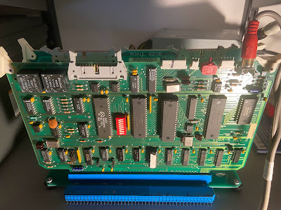
Here is the final product, a relatively clean looking 1 MiB EXORBus RAM and 3xVIA I/O card working great with the CMS 9619 and OS9 Level 2 on the CMS 9639:

Sunday, March 27, 2022

MIKUL 6809-5 Keypad

I received some membrane keypads in the mail today. Unfortunately, I neglected to order the 4x5 Keypads I hoped to use and only ordered 4x4 and (accidentally) 3x4 keypads. No problem. The 4x4 keypad will work fine to navigate the menus, with: * as clear; # as enter; D as Main Menu. You can't quite set the clock though because it is missing the keys to select year/month/day as they are on the missing row.

Here is the pinout, which requires a small jumper board to connect to either a 4x4 or 5x4 keypad, as the P3 header is not arranged in a very logical way:

  MIKUL 6809-5        eBay    |   Alltronics
   P3 HEADER       4x4 Keypad |   5x4 Keypad
        ___ 
COL1   |1     ->   3 - ROW3   |   6 - ROW3
ROW1  ||2     ->   5 - COL1   |   5 - COL3
COL2  ||3     ->   2 - ROW2   |   2 - ROW2				
ROW2  ||4     ->   6 - COL2   |   7 - COL4
ROW3  ||5     ->   7 - COL3   |   9 - COL5
ROW4  ||6     ->   x - N/C    |   3 - COL2
COL3  ||7     ->   1 - ROW1   |   8 - ROW1
ROW5  ||8     ->   8 - COL4   |   1 - COL1
COL4   |9     ->   4 - ROW4   |   4 - ROW4
       |___      

I think these are the orignial keypads that came with the TEMPMATE and CASEMATE firmware (pics from various auction sites):

Unfortunately, I think the cheap ebay 4x5 keypads I hoped to use will not work because they have 5 rows when the MIKUL's TEMPMATE software is written to use a keypad with 5 columns.

I found a keypad at Alltronics that has the right layout for only a few dollars. That keypad only has the flat flexible cable without a PCB connector, so I had to source that too. Also, it does not have the nice clicky metal domes in it so it feels mushy, but it works, and I can finally set the clock!:

Saturday, March 19, 2022

MIKUL 6809-5 Memory Map

By using the HCF instruction and a cheap logic analyzer, I was able to make a memory map of the MIKUL 6809-5:


External
 
FFFF


MEMORY OR I/O

EC00
EXTERNAL I/0 EBFF
EB10
U21 6821 PIA EB00-EB0F
EXTERNAL I/0 EAFF
EA10
U20 SIO/2 EA00-EA0F
U25 VRAM

MEMORY?
E9FF


E800

External
E7FF


MEMORY


0000

Of course, this lines up well with the MIKUL 6218 memory and VIA board. I need to update that memory map using the HCF technique.

Wednesday, March 16, 2022

MIKUL 6809-5 Processor and Video Board

I recently procured another EXORbus processor board, the MIKUL 6809-5, for a reasonable price. Let's take a look...

Notable ICs:

  • Motorola MC6809 processor
  • MC6821 Peripheral Interface Adapter (PIA)
  • MC6847 Video Display Generator (VDG)
  • Z0844206 SERIAL INPUT/OUTPUT CONTROLLER (SIO/2)
  • MM74C923 20 Key Keyboard Encoder

Ports:

  1. EXORbus card edge
  2. RS232 and RS485 / multidrop LAN port?
  3. 20 key matrix keypad
  4. LED indicator ?
  5. video output
  6. composite video

It is interesting that the board uses the MC6809 CPU with a MC6847 VDG like the Radio Shack Color Computer (CoCo). Unike the CoCo, it does not have an MC6883 SAM, making it similar to the Radio Shack TRS-80 MC-10 (which uses an MC6803, rather than the MC6809). So the basic CPU and video chipset places it somewhere between those two computers.

Notably, the board does not have any provision for ROM or application RAM on it. As a result, it needs another memory board on the bus to function properly. The MIKUL 6218 would make a perfect companion for it, but I already modified my 6218 board to work with the my CMS processor boards...whoops. So, with the price of these MIKUL boards dropping due to an apparent glut of them, I picked up a fresh MIKUL 6218 for ~$35 and installed them both in my EXORbus MULTI-PLANE backplane.

Despite the interesting video output, I am not in love with the features. The MC6821 PIA is dedicated to running the keypad encoder and baud rate dip switches, so it can't be used for much. Really the MIKUL 6809-4 or 6809-6 (Motorola MicroModule clone?) would be a better choice as a all-in-one SBC. However, the 6809-5s are definitely more pentiful and far cheaper right now, so maybe somebody else can make use of any info I publish about it.

More details below...

Wednesday, June 16, 2021

MIKUL 1MiB Mods (continued)

With the virtual address jumper for the MIKUL 6218 sorted, I still needed to simplify the address decoding and memory chip selects so that 1 of the 4 SRAM sockets will be selected depending on the state of our virtual A19 and A20 addresses. Since the three I/O ICs (6522 VIAs) share the data bus with the memory, I also need to disable the memory when the I/O is active, and signal the GAL in U10 to select the appropriate 6522 VIA.

Fortunately, the CMS 9619 and 9639 use several signals (VMA, VUA, or UTIL_DECODE) to indicate when the processor board is addressing external memory or I/O. This greatly simplifies the decoding from the original MIKUL arrangment which had the GAL fully decoding all of the address lines from A6 through A15. But, since the MIKUL 6218 board does not use those CMS/EXORbus decode signals, I had to cut a few of the unneeded low address lines to the GAL and replace them. With this simplified arrangement, I had hoped to use a few standard 74LS logic ICs to select the RAM and I/O. But, after a few attempts reduce the number of logic chips I needed, I decided to bite the bullet and just get a GAL programmer.

Here is my new setup which seems to work great with macOS:

  • XGecu TL866II plus USB programmer - programs the GAL
  • minipro - reads and writes JDEC files to the TL866
  • GALasm - turns logic equations into JEDEC file
The biggest obstacle was that the first programmer I ordered (an older model TL866A) did not work due to a faulty pin 10. Unfortunately, this has been my luck with new tech items from China, including the cheap logic analyzer I bought a while back. These kinds of issues take A LOT of time to figure out.

Once I received a functioning programmer, I managed to get everything working well with my CMS 9619. So, now I can switch in 16 blocks of 32K RAM (512K) into the lower half of the CMS9619 address map, using the low nibble of its PIA output (at $FFC4) as a register to drive the virtual address lines. The CMS 9619 does not output a signal on its PIA for A20, so I can only use 2 of the SRAMs. Also, since the RAM addresses overlap the CPU addresses, half of each 512K SRAM chip can't be accessed (when A15 is high). This could be easily fixed by modifiying the U13 jumper board that I made previously, or even the CMS 9619 address decoder. Honestly, the original configuration was probably better for the CMS 9619 because it did not switch out the lower 8K of RAM that an OS would use. However, since my end goal is to use this with the CMS 9639 CPU and its integrated MMU, I will keep it as-is. I haven't fully tested the I/O and the VIAs yet, but I will get to those soon enough.

512K RAM on a MC6809!
Note the rainbow virtual address jumper and the
additional jumpers to route A19 and A20

More of the techincal details below, after the break...

Wednesday, April 21, 2021

MIKUL 1MiB Mods

A18 Addition

I really want to use my two 512KiB SRAM chips on this board to maximize the usable RAM. Fortunately, the MIKUL 6218 has 32 pin DIP sockets, so my SRAM physically fits. However, pin 1 (A18) of the socket is connected to VCC, limiting each socket to 256KiB (2^18) of memory. This is strange because four 256KiB (2MBit) SRAM chips would be perfect for this board (and my needs) but are quite unusual and are actually more expensive than four 512KiB (4MBit) SRAM chips.

To increase the socket capacity to 512KiB, the trace connecting A18 to VCC for each memory chip must be cut. Unfortunately, this is a wide power trace that is hidden under the end of the sockets. A few seconds with an 1/8" drill at a 45° angle cut through the A18 pull-up trace without too much collateral damage. Although I slightly cut into the socket, I barely avoided cutting into the next thin address line down.  

A18 to VCC severed.

Then, I added a few wire jumpers to connect pin 1 of each socket to each other to give a common A18 line. This address line, along with A16 and A17, need to be connected to a new virtual address header. A19 and A20 will be connected from this header to a decoder to create the memory chip select signals.

Bank Address Eliminator

With the physical connections made, it's time to simplify the MIKUL 6218's memory bank select system.

This little jumper board just connects each real address to its respective memory address line (A11-A15), overriding the bank switching latch and logic at U13. The virtual addresses (A16-A20) connect to the 10 pin header which will connect to the main CMS 9639 processor board. The 3 pin header on the right will connect A19 and A20 to a decoder to select the correct memory chip.

With the RAM and this board in place and the virtual address lines pulled high, the board works exactly the same way as it did before and has the same memory map. However, the bank register functionality (which I could not test anyway) has been eliminated. But, without the virtual addresses, I can only access some of the RAM.

Next time ... the RAM chip select Decoder

Sunday, January 3, 2021

MIKUL 6218 Memory and VIA EXORbus board

I haven't spent much time working on my CMS 9639 SBC because, unlike the CMS 9619, it does not have any usable on-board RAM and does not include a monitor/debugger in ROM. Instead, it is designed to use an external memory board (which I don't have) on a back plane (which I now have) and boot OS-9 from a disk drive (which I don't have). What is nice about the device is the built-in memory manager which uses up to 1MiB of RAM. Unfortunately, EXORbus RAM cards are still prohibitively expensive on eBay and only have 16K to 64K of RAM capacity. Since the components would be far less than the price of those boards, I took a stab at designing a 1MiB SRAM board with a bonus additional I/O expansion.

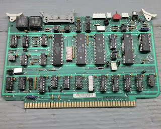
I had just started to get components inserted into an EXORbus prototype board when I noticed the MIKUL 6218 Memory and VIA boards appearing on eBay at reasonable prices (<$45 shipped). Let's take a look at the board:

Click below for more details...