I ran jumpers wires on the back of the Apple II+ logic board to route the various signals I needed (PHI_0, AX, A14&A15) to the J1 socket area. Fortunately since only half of J1 is used by the Apple II+, I can use the unused pins of that socket to route my signals through to the new circuit I am adding.
Here is my circuit diagram:

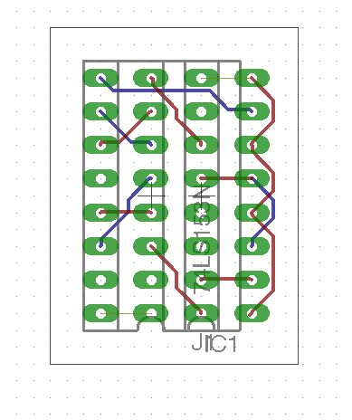
and the adapter board:
Warning - I don't know if this works yet.
After I ran the wires, I started trying to solder a tiny adapter board to translate the 74LS257 signal locations to the new 74LS153 IC. That was taking too much time for something that might not work at all, so I put the circuit on a bread board. Here it is:

Unfortunately, this did not work. I suspect that the dip jumper cable may be too long and adding some capacitance or delay. Or, the RAM timing may have been thrown off by the internal logic of the new IC. My Apple II+ is not booting and is in a similar state to when the RAM was in the wrong row. I'm sure I would have figured this out, but Halloween took priority.
Better news is that my Apple IIb is in a pretty final state. I think I will start buying supplies to actually build it.

Until next time, RetroChallenge!
I like this idea. I also have an Apple 2+ motherboard just lying around doing nothing. (We seem to have a lot of similar circuit boards.) What I've considered doing with mine is making a faux Apple 2 clone by putting pirated ROMs into a real Apple motherboard, and then putting that board in a generic case of some sort. Not sure what I'll do for a keyboard or disk drives yet, but I have a couple broken 2cs (and 2 good ones) and maybe I could use drives (and possibly a keyboard) borrowed from them.
ReplyDelete