Replacing the RAM in my Apple II+ has become a bit of a project in and of itself. Sure I could just buy some 4116 (16K bit)
DRAM, but that's not very exciting, and its not an upgrade. So, Instead, I have been figuring out how I can use 4264 (64K bit) DRAM in its place. There are a lot of considerations that need to be made including power, refresh circuit, and addressing the new RAM. The descriptions below are for an RFI Revision 01 board, and may be different for other revisions. Click below to see the details of re-routing the RAM power lines and my preliminary results.
Power
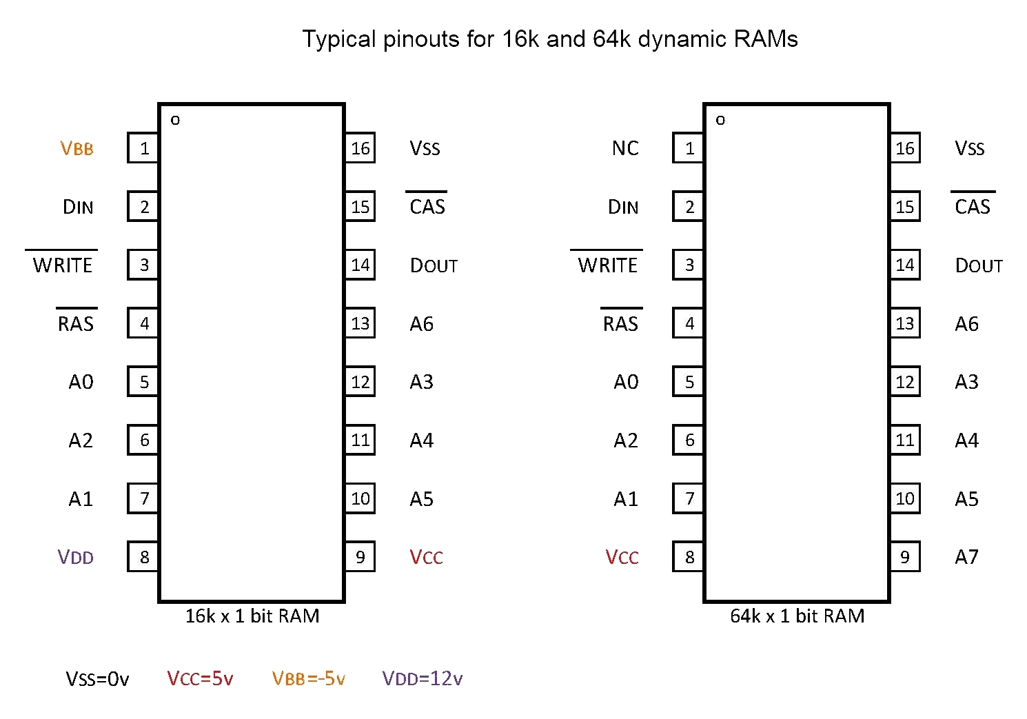
I tried a number of possible ways to get the correct power to the 4264 DRAM ICs. Here is a good image that shows the differences in the power requirements between the two types of ICs:

| Basically, the power for the 4264 DRAM is simpler. There is no need for the -5v power, or the +12v power, and the +5v power moves to the former +12v power pin. There are a number of sites online that show how to do this, but generally just as a 16K RAM replacement, rather than enabling 64K RAM.
|
Disabling pin 8 +12v VDD
I tried disconnecting and cutting the main +12v rail near the bottom of the logic board and putting a +5v lead on it, but the timing generator at the bottom of the board also needs +12v power. I had to add a long wire down the side of the board to get the +12v power down there. I didn't like that solution and repaired it. I tried cutting the +12v bus at the vias, but the tracks are too thick and I was worried I would do a lot of damage. Instead, I lightly drilled into the
vias that connect the main +12v rail to each the RAM rows. You need to drill all three of the vias before they are isolated since they are also connected to each other at the sixth RAM chip.
Disabling pin 1 -5v VBB
The RAM gets -5v from pin 34 of peripheral slot 4. Cut this trace to disable the power to the RAM. It probably does not need to be cut for most 4264 DRAM chips as this pin is generally a
"NC". On some chips it defines the refresh, or the page mode, so I just cut it.
Disabling pin 9 +5v VCC
The trace for +5v comes from pin 23 of the D8 ROM. I cut that trace too. Again, you could get away with leaving it if all you wanted was a 16K RAM replacement, but I'm shooting to use most, if not all, of the 64K RAM that I will have.
Re-Routing +5v VCC to pin 8
I added a short jumper wire from pin 23 of the D8 ROM to pin 8 of a RAM chip in the first RAM row. That is sufficient to distribute the power to all of the RAM. Many websites show do this by not disconnecting the +5v from pin 9, and adding a jumper across to pin 8, but this only allows you to use 16K of the new RAM chips. For now, I added the jumper on a socket that will be easy to remove later. This will keep the A7 pin from floating. That way I can test all my modification thus far. Unfortunately, I will only be able to use the highest 16K of RAM that way.
Early Results
Finally, I quickly turned the computer on and off with no RAM. No smoke, so I left it on for pictures. A screen full of question marks. At least the character ROM, clock and video scanner seem to be working. This looks promising!


No comments:
Post a Comment